Making a printed circuit board (PCB).
- First cut the copper clad board to size required.
- Sand the surface of the board to remove the layer of copper oxide that is formed due to the reaction of the copper with the oxygen in the air.

- Once the copper surface is shiny and clean avoid touching the surface of the copper.
- Eaglecad or ORCad may be used to design the schematic and the pcb design .
- Take a mirror image of the pcb design while using the CAM processor to generate the Gerber files .
- The gerber files maybe viewed online at http://www.circuitpeople.com or the .eps file maybe viewed offline using the .eps viewer take a lazer printout of the pcb layout using. this printout will be the mirror image of the actual pcb layout .
- Since during the transfer process the mirror image of the actual image will be transferred.
- Now cutout the actual PCB layout on the transperency. this will be the toner transfer
- .
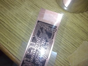
- Lightly wipe the toner layer of the toner transfer with a peice of cloth and the surface of the cleaned copper clad. This will ensure that there is no dust or grime between the toner surface and the copper.
- Place the transfer on top of the cleaned copper clad board.
- Secure the layout in place with the help of a peice of tape or some glue.
- Using a hot clothes iron heat the toner transfer so that the toner layer from the tranfer is transferred onto the copper.(set the iron to the highest temperature possible…usually the cotton settings)
- Iron the transperency gently.
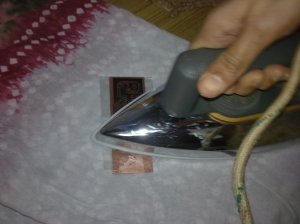
- Don’t put too much pressure on the clothes iron else the toner will smudge. too little pressure and the toner wont be transferred at all.
- Once you think the toner is stuck to the copper turn off the iron. let it cool down to the ambient temperature.

- Peel off the transperency if you got it right then you will see that almost all the toner has been transferred to the copper surface.
- The toner layer will form the etch resist.
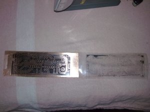
- Now the copper clad can be put into the etching tank. ferric chloride maybe used as the etchant. although muriatic acid maybe used too.
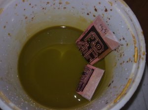
- Gently ‘move’ the copper clad board through the FeCl3 solution.
- Once all the unwanted copper has been removed clean the PCB under running water.

- Remove the layer of the toner with some sand paper or a solvent such as acetone.
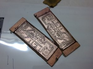
- If the PCB is meant for surface mount components then the PCB might require drilling.
- After the drilling is over. tin the copper surface to protect and increase the conductivity of the copper tracks.
References:
http://www.riccibitti.com/pcb/pcb.htm
http://www.fullnet.com/~tomg/gooteepc.htm
http://www.youritronics.com/diy-printed-circuit-board-using-photo-etching-method/